
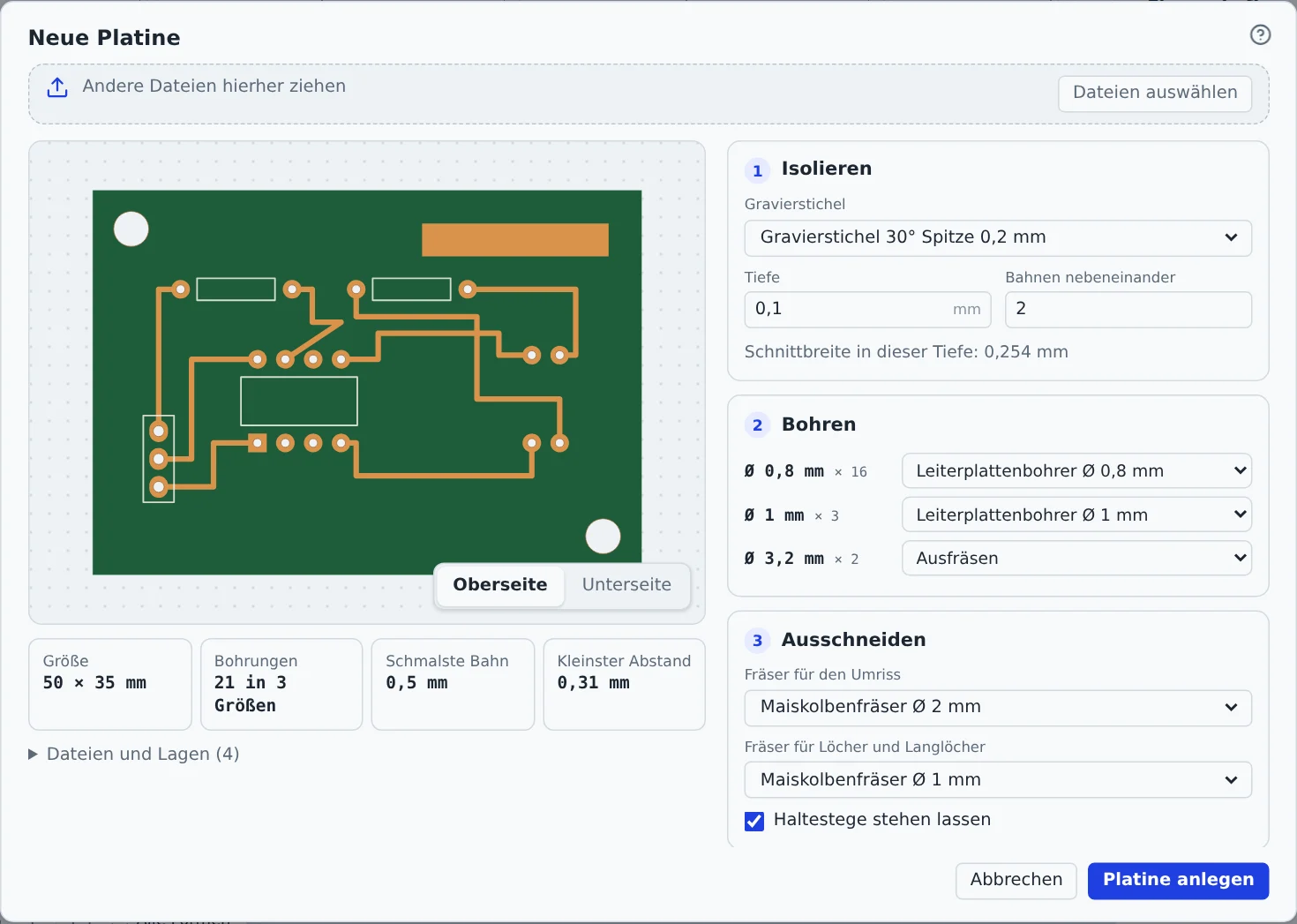
From the manufacturing files of your schematic program, the app mills a single-sided board in three steps: Isolate (a fine engraving bit separates the traces from each other), Drill and Cut out.
Reading the files
Choose File → New → Circuit board or the Circuit board (Gerber) card in the “Import” window. Then drag the ZIP with the manufacturing files or single files into the window. Gerber and drill files dropped straight onto the canvas open the window as well.
The app reads Gerber (RS-274X with X2 attributes) and Excellon drill files from KiCad, EasyEDA, Eagle, Altium and Fritzing. It recognises each layer by content and file name. Under Files and layers you can change any assignment or leave a file out with “Don't use”.
If the outline is missing, the app estimates the edge from copper and holes with a 2 mm margin. The preview then shows it dashed.
Choosing the side
If the board has copper on both sides, choose Top or Bottom below the preview. Each side is its own project. The bottom appears mirrored, the way it lies on the machine after flipping.
Isolating
A V-shaped engraving bit mills around every copper area. The width of the cut depends on tip, angle and depth. The window shows the cut width for the chosen depth. Passes side by side (1 to 5) widens the gap between traces, which makes soldering easier.
The most robust bit whose cut width still fits between the closest traces is preselected. Narrow spots marked in red are smaller than the cut width; traces stay connected there. Choose a finer bit or less depth. A depth of 0.05 to 0.1 mm is common, as the copper is usually only 0.035 mm thick.
Drilling
For each diameter the app suggests a matching drill from the library. Similar diameters share one drill. Holes without a matching drill (such as mounting holes) and slots are milled. Choose a thin cutter for them under “Cut out”.
Cutting out and blank board
A corn cob cutter cuts the board out along its edge. Holding tabs keep it in place until the end. Cutouts inside the board are milled along their inside. For the blank board, enter the thickness (usually 1.6 mm) and the margin around the board.
The finished project
Create board adds the layers “Isolate copper”, “Drill Ø …” for each drill, “Mill holes”, “Cut outline” and the hidden “Silkscreen” for orientation. The material is a circuit board with matching cutting data. In the Cutting tab each cutter is its own program, in the right order.

Stick the blank board fully onto a flat spoil board with double-sided tape. Even a tenth of a millimetre of warp makes the isolation cuts uneven. Probe Z again after every tool change, see Probing Z.
Height probing
Hardly any blank board lies perfectly flat. A tenth of a millimetre of warp is enough for the bit to leave copper connected in one place and cut too deep in another. That is why the machine probes the board in a grid before isolating.
- Set the origin as usual and probe Z on the board.
- Attach one clip to the engraving bit and the other to the copper of the blank board. The bit itself is now the probe.
- Choose Machine → Height probing … or Height probing in the machine panel, then Start probing.
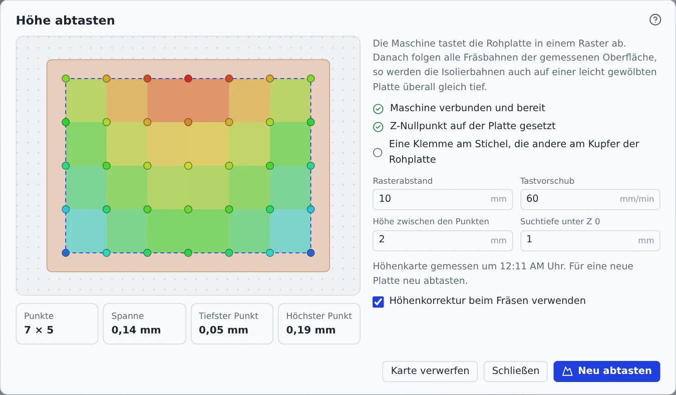
The machine visits the points in a snake pattern, covering the toolpaths plus a small margin. The map shows low spots in blue and high spots in red; below it you see the lowest and highest point and the range between them. With Use height correction when cutting switched on, every toolpath follows the measured surface. Long moves are split into 1 mm pieces for this, and values between grid points are interpolated.
The map belongs to the clamped board and stays in the browser until you probe again or discard it. If the range is more than 0.5 mm, the board probably does not lie flat; stick it down again. After a tool change, probe Z at the same spot as before, and the map still fits.